

At CES 2026, Intel unveiled the Core Ultra Series 3 processors—codenamed Panther Lake—marking the first consumer chips manufactured on the company's highly-anticipated 18A process node. This launch represents far more than a routine product announcement; it's the culmination of years of technical challenges, strategic pivots, and billion-dollar bets that could determine Intel's viability as a leading-edge semiconductor manufacturer.
What Intel Announced: Core Ultra Series 3 Specifications
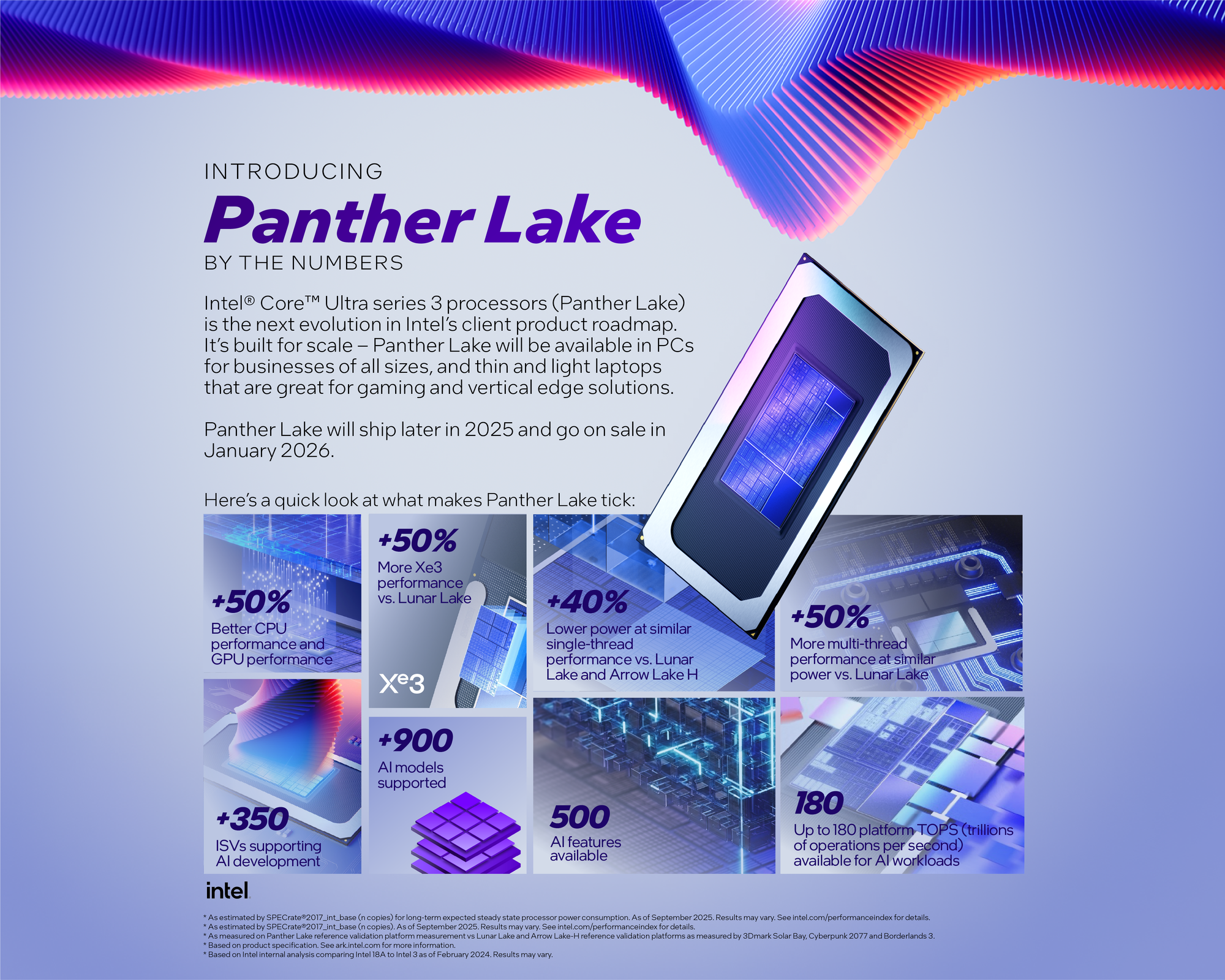
Intel's Core Ultra Series 3 lineup consists of 14 SKUs spanning multiple performance tiers, with global availability beginning January 27, 2026. The lineup introduces a new X-series designation for premium configurations, fundamentally restructuring how Intel segments its mobile processor portfolio.
The X-Series Flagship: Core Ultra X9 388H
The headlining Core Ultra X9 388H represents Intel's most aggressive integration of computing resources in a mobile processor to date. The chip features up to 16 CPU cores in a hybrid architecture: four performance cores, eight efficiency cores, and four low-power efficiency cores. This configuration departs from the P-core-only approach of Lunar Lake, returning to the heterogeneous architecture that characterized Meteor Lake.
The GPU subsystem receives particular attention with the Arc B390 integrated graphics, featuring 12 Xe3 cores—a substantial increase over previous generation integrated graphics. Intel claims the Arc B390 can match discrete RTX 4050 performance in gaming scenarios, a bold assertion that positions integrated graphics as a legitimate alternative to entry-level discrete solutions.
AI capabilities center on a 50 TOPS neural processing unit, maintaining parity with Lunar Lake's AI acceleration while the rest of the platform scales performance substantially higher. The chip supports both LPDDR5x and DDR5 memory depending on OEM configuration, though X-series models exclusively use LPDDR5x for power efficiency.
Performance Claims and Competitive Positioning
Intel's performance assertions position Panther Lake as a significant leap from its predecessor. The company claims up to 60% better multi-threaded performance compared to Lunar Lake's Core Ultra 9 288V in Cinebench 2024, both chips running at 25W. Gaming performance supposedly improves by up to 77% generation-over-generation, measured across 45 game titles at 1080p with 2x upscaling.
Battery life projections reach 27.1 hours during Netflix streaming on the Core Ultra X9 388H in Lenovo's reference design—impressive figures that would position Panther Lake competitively against both AMD's Ryzen AI Max (Strix Halo) and ARM-based alternatives.
Intel's new XeSS3 frame generation technology enables the GPU to render three AI-generated frames for every GPU-rendered frame, potentially transforming perceived performance in supported titles. This places Intel's integrated graphics in direct competition with NVIDIA's DLSS ecosystem, though real-world implementation quality will determine whether Intel's solution achieves comparable results.
The Broader Lineup: H-Series and U-Series Configurations
Beyond the X-series flagships, Intel's Core Ultra Series 3 includes traditional H-series and U-series variants. H-series chips can turbo up to 65W or even 80W, while non-H parts top out at 55W, creating clear thermal and performance boundaries for OEM system designs.
The lineup also introduces mainstream Intel Core processors based on the same Panther Lake architecture but positioned at lower price points. This bifurcation allows Intel to address both premium and mainstream segments while maintaining architectural consistency across the product stack.
The 18A Manufacturing Process: Technical Innovation Under Pressure
Panther Lake's significance extends beyond processor specifications to the underlying manufacturing technology. The 18A process node—Intel's 1.8nm-class technology—represents the first production deployment of two fundamental innovations that Intel has promoted for years: RibbonFET gate-all-around transistors and PowerVia backside power delivery.
RibbonFET: Intel's Gate-All-Around Implementation
RibbonFET transistors represent Intel's implementation of gate-all-around (GAA) architecture, a transistor design that provides superior electrostatic control compared to traditional FinFET structures. By wrapping the gate material completely around the channel, GAA transistors reduce leakage current and enable better performance at lower voltages—critical advantages for mobile processors where battery life directly impacts user experience.
Gate-all-around technology has been an industry focus for years, with Samsung and TSMC pursuing their own implementations. Intel's simultaneous deployment of both GAA and backside power delivery in a production node represents an aggressive approach that carries significant risk. Typically, semiconductor manufacturers introduce major innovations sequentially to reduce complexity and improve yield learning curves.
PowerVia: Rethinking Power Delivery
PowerVia, Intel's backside power delivery network, fundamentally reorganizes how electrical power reaches transistors. Traditional semiconductor designs route both signal and power connections on the same side of the silicon wafer, creating routing congestion that limits design flexibility and signal integrity.
By moving power delivery to the backside of the wafer, PowerVia frees up frontside routing resources for signals, reduces power delivery resistance, and improves overall power efficiency. Intel claims this enables approximately 15% better performance per watt compared to traditional power delivery approaches—a significant advantage in power-constrained mobile designs.
The innovation required substantial changes to Intel's manufacturing processes, including modified wafer handling, new lithography approaches, and entirely different packaging methodologies. The technical complexity explains why TSMC's comparable technology, expected in its N2P node, won't arrive until potentially a year after Intel's implementation.
Process Node Positioning: 18A vs. TSMC N2
Intel positions 18A as competitive with or superior to TSMC's N2 node, which is scheduled to enter high-volume production in late 2025. Transistor density metrics show rough equivalence between the two processes, though Intel claims its PowerVia implementation provides performance and efficiency advantages that pure density measurements don't capture.
The competitive landscape becomes more complex when considering that TSMC's N2 reportedly achieves 90% yield rates in pilot production, while Intel's 18A yields have been a source of speculation and concern. Yield—the percentage of functional chips produced from each silicon wafer—directly impacts manufacturing economics and the ability to meet customer commitments at competitive pricing.
The Turbulent Path to 18A: Five Nodes in Four Years
To understand Panther Lake's significance, it's essential to examine the broader context of Intel's manufacturing roadmap and the strategic decisions that led to this moment.
Pat Gelsinger's Audacious Gambit
When Pat Gelsinger returned to Intel as CEO in February 2021, he inherited a company that had fallen behind in process technology—an existential crisis for a manufacturer that built its reputation on leading-edge silicon. Gelsinger's response was the "Five Nodes in Four Years" strategy, an unprecedented acceleration designed to regain process leadership from TSMC.
The roadmap called for delivering Intel 7, Intel 4, Intel 3, Intel 20A, and Intel 18A between 2021 and 2025. This aggressive schedule required massive capital investment, intense R&D focus, and the willingness to push manufacturing teams through overlapping development cycles with minimal recovery time between nodes.
The strategy embodied in Gelsinger's IDM 2.0 vision sought to position Intel both as a competitive chip designer and as a viable foundry alternative to TSMC for external customers. Success would validate Intel's continued vertical integration, while failure would likely force the company to split its design and manufacturing operations—a possibility Gelsinger explicitly rejected when accepting the CEO role.
The 20A Cancellation: De-Risking or Red Flag?
In August 2024, Intel announced it would cancel the 20A node for high-volume production of Arrow Lake processors, instead relying on external foundries—likely TSMC—for those chips. Intel framed the decision as a success: the company's "sooner-than-anticipated" progress on 18A made 20A redundant, allowing resource reallocation to the more advanced node.
The cancellation saved Intel approximately $500 million while theoretically accelerating the transition to 18A. However, industry observers noted that 20A served a critical de-risking function. The node was designed to introduce RibbonFET and PowerVia on a less complex product before scaling to 18A's more demanding requirements. Skipping that learning step meant Intel would simultaneously introduce both technologies at volume on 18A—a high-risk approach that left no fallback if problems emerged.
The decision occurred against a backdrop of significant financial pressure. Intel posted a $1.6 billion net loss in Q2 2024, triggering a restructuring plan that included eliminating more than 15,000 jobs, cutting R&D and marketing spending, and reducing capital expenditure by 20%. The company needed to optimize resource allocation, and 20A became an acceptable casualty in service of that goal.
Customer Concerns and Yield Challenges
Throughout 2024 and 2025, reports emerged suggesting that potential foundry customers expressed concerns about 18A readiness. Broadcom reportedly received test wafers from Intel's 18A process and concluded the technology wasn't yet viable for high-volume production. Nvidia, positioned as a key potential customer through a $5 billion partnership announced in September 2025, delayed production trials citing unresolved technical issues.
These setbacks raised questions about whether Intel could simultaneously execute on its internal product roadmap while building the credibility necessary to attract foundry customers. The company found itself in a catch-22: it needed external customers to justify continued foundry investment, but potential customers demanded proof of execution before committing to Intel's processes.
Yield challenges compounded the credibility problem. While Intel claimed defect densities had improved to acceptable levels (reportedly below D0 <0.40), the fact that major customers expressed disappointment suggested real-world yields might lag behind Intel's internal metrics or that performance variability remained problematic.
Leadership Transition: From Gelsinger to Tan
In December 2024, Intel announced Pat Gelsinger's retirement, effective immediately. The abrupt nature of his departure—characterized by some reports as a forced exit—signaled board dissatisfaction with the pace and direction of Intel's turnaround. Gelsinger's replacement, Lip-Bu Tan, brought a different perspective as the former CEO of Cadence Design Systems, a major electronic design automation company.
Tan's early statements as CEO suggested potential strategic shifts. Reuters reported in mid-2025 that Tan was considering deprioritizing 18A for external foundry customers, instead focusing resources on the next-generation 14A node expected in 2027-2028. Such a pivot would effectively withdraw Intel from the foundry market for several years while TSMC and Samsung continued advancing their roadmaps.
The speculation raised concerns about potential write-offs. Intel had invested billions in 18A development, and abandoning external sales would require accounting for those investments as losses—potentially hundreds of millions or even billions of dollars in charges that would further pressure Intel's financial position.
However, by late 2025, Intel's messaging stabilized. The company announced 18A had entered risk production in April 2025—a critical milestone indicating the technology was ready for initial low-volume manufacturing runs. By October 2025, Intel confirmed high-volume production had begun at Fab 52 in Arizona, with Panther Lake chips slated to ship before year-end.
What Panther Lake's Launch Means for Intel's Future
The Core Ultra Series 3 launch represents Intel's most consequential product introduction in years, with implications extending far beyond the mobile PC market.
Proving Manufacturing Viability
First and foremost, Panther Lake must demonstrate that Intel can successfully manufacture a complex, leading-edge processor on its most advanced node. The chip needs to meet performance claims, achieve acceptable yields, and ship in volumes sufficient to satisfy OEM commitments across more than 200 planned designs.
Success would validate the billions invested in 18A and potentially attract the foundry customers Intel desperately needs. Microsoft has publicly committed to using 18A for custom chips, providing an important credibility boost, but landing additional customers like Nvidia, Qualcomm, or AMD would transform Intel Foundry from a theoretical business into a viable TSMC alternative.
Failure—whether through yield issues, performance shortfalls, or delayed availability—would confirm skeptics' concerns that Intel attempted too aggressive a technical leap. Such an outcome could accelerate discussions about spinning off Intel's manufacturing operations or accepting a reduced role focused solely on internal products.
Competitive Positioning in Mobile Computing
From a product perspective, Panther Lake faces intense competition across multiple dimensions. AMD's Ryzen AI Max series (Strix Halo) offers substantially more compute resources by integrating up to 16 RDNA 3.5 GPU cores, positioning those chips for creator and gaming workloads that demand maximum performance regardless of power consumption.
Apple's M-series processors continue advancing on TSMC's leading-edge nodes, with the M4 family already demonstrating the performance and efficiency advantages of integrated design executed on world-class manufacturing. Qualcomm's Snapdragon X Elite and upcoming Snapdragon X2 Elite Extreme bring ARM architecture to Windows, challenging x86's traditional dominance with claims of superior power efficiency.
Intel's advantage lies in its x86 ecosystem compatibility, extensive OEM relationships, and the potential for competitive pricing if 18A yields improve. The company has over 200 PC designs committed to Panther Lake, suggesting OEMs maintain confidence in Intel's execution—though many of those same OEMs hedge their bets by offering AMD and Qualcomm alternatives within the same product lines.
The Embedded and Edge Computing Opportunity
Intel's expansion of Core Ultra Series 3 into embedded and industrial use cases represents a strategic diversification beyond traditional PC markets. Certifying processors for extended temperature ranges, 24x7 reliability requirements, and long-term availability commitments opens opportunities in robotics, smart cities, healthcare, and industrial automation.
These markets typically value stability, longevity, and ecosystem maturity over cutting-edge performance, potentially playing to Intel's strengths while reducing dependence on the volatile consumer PC market. If Intel can establish itself as a reliable edge computing platform provider, it creates a revenue stream less susceptible to quarterly PC shipment fluctuations.
The company claims significant advantages in AI workloads versus NVIDIA's Jetson Orin AGX platform, including 1.9x higher large language model performance and 4.5x higher throughput on vision language action models. These figures, if validated by independent testing, would position Intel competitively in the rapidly-growing edge AI market where local processing increasingly complements cloud-based inference.
The Foundry Question Remains Unanswered
Despite Panther Lake's successful launch, Intel Foundry's viability as a business remains uncertain. The division generated $4.4 billion in revenue in Q2 2025, but the vast majority came from manufacturing Intel's own chips. External customer wins remain limited, with Microsoft representing the most significant publicly-announced commitment.
Tan's July 2025 statement that Intel might abandon the foundry business entirely if external customers don't materialize underscores the strategic crossroads the company faces. Developing next-generation process nodes requires sustained multi-billion-dollar investments with long payback periods. Without external customers to share development costs and utilize excess capacity, the economic case for continued foundry investment weakens considerably.
The U.S. government's CHIPS Act funding—Intel received $8.9 billion in federal support—creates political pressure to maintain American semiconductor manufacturing capabilities. However, government subsidies can't indefinitely sustain a business without commercial viability, and competitors like TSMC are also building U.S. facilities that could fulfill national security objectives.
Technical Excellence Isn't Enough
Intel's Core Ultra Series 3 represents impressive engineering achievement. The simultaneous introduction of gate-all-around transistors and backside power delivery in a production mobile processor demonstrates technical capability that rivals or exceeds competing foundries' roadmaps. The product specifications, if validated by independent testing, position Panther Lake competitively across performance, efficiency, and battery life metrics.
However, Intel's challenges extend beyond technical execution to encompass market positioning, customer credibility, financial sustainability, and strategic clarity. The company must simultaneously satisfy multiple constituencies: PC OEMs demanding reliable high-volume supply, potential foundry customers requiring proof of manufacturing consistency, investors seeking profitability and growth, and employees navigating organizational restructuring and strategic uncertainty.
Panther Lake's success in the market will provide crucial data points. Do the performance claims hold up in independent reviews? Can Intel ship in the volumes OEMs require? Will consumers choose Panther Lake systems over AMD, Qualcomm, or Apple alternatives at comparable price points? Do the chips maintain their promised efficiency characteristics across diverse workloads and real-world usage patterns?
The answers to these questions will determine whether 18A represents the foundation for Intel's manufacturing resurgence or an expensive proof point that technical achievement alone can't overcome years of lost momentum and diminished market position. For Intel, Panther Lake isn't just another product launch—it's validation that the billions invested and jobs eliminated in pursuit of manufacturing leadership might actually pay off.
The semiconductor industry will be watching closely, because if Intel succeeds, it demonstrates that even fallen giants can recover through sustained investment, technical innovation, and willingness to make difficult strategic choices. If Intel stumbles, it confirms that manufacturing leadership, once lost, may be impossible to reclaim against entrenched competitors with superior execution track records and customer trust.
Either way, the Core Ultra Series 3 launch marks a pivotal moment not just for Intel, but for the broader question of whether American semiconductor manufacturing can compete at the leading edge in an era increasingly defined by geopolitical competition and supply chain resilience concerns. Panther Lake's fate will echo far beyond quarterly earnings reports and product reviews, potentially shaping the semiconductor industry's structure for the next decade.


Discussion